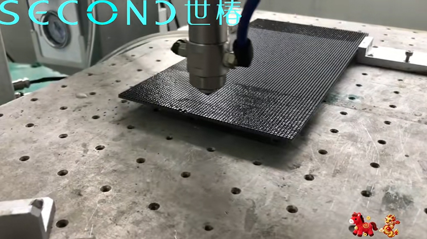
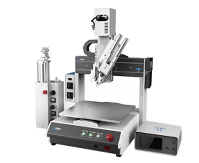
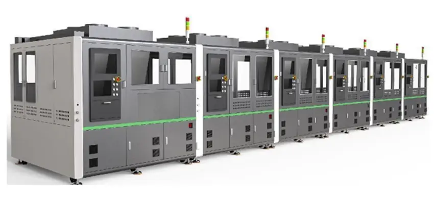
With the rapid iteration of Mini/Micro LED display technology, full-color LED screens are evolving towards smaller pitch, higher density, and superior image quality. In this process, dispensing encapsulation is no longer a simple physical protection step, but a core element determining the uniformity of light output, color mixing consistency, and long-term reliability of the screen. How to solve common problems in full-color LEDs such as “screen flickering,” “pigmentation,” and “color shift” through dispensing has become a key issue in the encapsulation process. This article will delve into the technical challenges of uniform light dispensing in full-color LED screens and provide practical solutions based on real-world application scenarios.
Uniform light dispensing for full-color LED screens” is not a single standard process name. It usually refers to a combination of precision dispensing and encapsulation technologies used to achieve uniform light output and eliminate color differences and light spots in full-color LED displays. Its core lies in using the optical design of the adhesive (such as lenses and diffusion layers) and precise molding control to make the light output of each pixel as consistent as possible
Ⅰ.Major Process Challenges in Uniform Light Dispensing
Achieving ideal uniform light distribution in actual production lines is not easy, mainly facing three physical and chemical challenges:
1.Differences in PCB Surface Flatness and Wetting Properties
The PCB board of a full-color LED module contains copper traces, pads, and solder mask layers, with micron-level height differences between these areas. Due to the different surface tensions of copper, gold, and the substrate material, the adhesive tends to accumulate in areas of low surface tension during the flow and leveling process, resulting in “white spots” (uncovered adhesive) or uneven thickness at the edges of pads or copper traces, thus affecting local light output. If organic contaminants are present on the surface, the adhesive may “crawl” or produce voids due to poor wetting properties.
2.Bubbles and Pitting Defects
Microbubble entrapment is unavoidable during dispensing and adhesive mixing. If bubbles remain above the chip or inside the adhesive layer, they will form black spots or scattering pits on the display screen after curing, severely reducing yield. Especially in small-pitch products, where the gaps between LEDs are extremely small (down to less than 0.5mm), air bubbles are more easily trapped in these narrow gaps.
3.Adhesive Layer Thickness and Surface Shape Control
The uniform light distribution effect is highly dependent on the optical surface shape of the adhesive layer. Insufficient adhesive can lead to exposed chips or insufficient light mixing distance; excessive adhesive may overflow onto the pads, causing poor contact, or create an excessively large radius of curvature, thus reducing light focusing ability. For large-size modules, ensuring that the overall adhesive layer thickness tolerance is controlled within ±0.1mm is a challenge in coordinating dispensing equipment and processes.
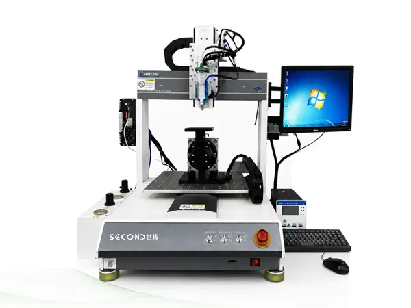
Desktop glue dispensing machine robot SEC-E480SV with CCD visual
Second Intelligent Desktop Glue Dispensing Machine SEC-E480SV adopts high-precision servo motor + grinding ball screw, which can ensure accuracy while having higher cost performance. It is also equipped with CCD visual height measurement, which makes programming more efficient and more accurate. It is an aviation aluminum alloy die-casting one-piece design desktop glue dispensing machine, which is more solid, more stable, with double rotating stations, small and flexible.
Ⅱ.Based on existing process data, LED dispensing solutions for achieving “uniform light” effects mainly fall into the following technical paths:
Path 1: Lens Dispensing This method involves applying transparent optical adhesive and allowing it to cure into a microlens, directly altering the light emission angle of the chip, thereby improving brightness and uniformity.
Process Key Points: A specific amount of transparent adhesive (such as silicone or UV adhesive dispensing machine) is precisely sprayed onto each LED chip dispensing machine. The surface tension of the adhesive or mold pressing is used to form a spherical or specific curvature lens. The key is extremely high adhesive consistency and concentricity. The deviation between the center of the adhesive dot and the center of the chip is typically required to be controlled within 0.1mm, and there should be no air bubbles in the adhesive to ensure consistent light focusing and luminous flux for each LED chip.
Applicable Scenarios: Commonly used in Mini LED backlighting or small-pitch full-color displays where high brightness and light pattern requirements are necessary.
Path 2: Dam & Fill For small-pitch or Mini LED full-color screens, to prevent light leakage between adjacent pixels (leading to uneven color), physical barriers are first constructed before filling.
Key Process Points: First, a “dam” (forming a grid) is drawn around the chip array or between pixels using high-viscosity adhesive. After curing, an encapsulating adhesive containing light-diffusing particles is filled into the grid. The width and height of the dam lines must be strictly controlled (e.g., line width 0.5mm ± 0.05mm), and there should be no protrusions at the intersections; otherwise, gaps and light leakage will occur after lamination. The filler adhesive is responsible for converting point light sources into surface light sources, achieving “uniform light.”
Path 3: Optical Adhesive Film/Diffusive Layer Mounting (Partially Replacing Dispensing)
For solutions requiring extremely high surface flatness and ease of rework, solid optical adhesive films are sometimes used instead of liquid dispensing.
Process Key Points: An optical adhesive film containing a white diffusion encapsulation layer and a black light-transmitting layer is applied to the LED board dispensing via molding or lamination. The white diffusion layer contains light-diffusing particles (transmittance controlled between 20% and 80%), responsible for evenly dispersing the LED’s point light; the black layer enhances contrast and color consistency. This effectively solves the color difference problem caused by uneven thickness in liquid dispensing during splicing.
III. Key Process Control Parameters for Full-Color LED Screen Dispensing?
Regardless of the path chosen, achieving “uniform light” requires strict control of the following aspects:
Adhesive Degassing: Vacuum degassing is essential before dispensing to prevent air bubbles in the adhesive from causing abnormal light scattering or localized dark areas after curing.
Surface Treatment: Plasma cleaning is often required before dispensing to improve the wettability of the substrate or support surface, preventing adhesive creep or uneven spreading.
Curing Strategy: For UV adhesives, matching wavelengths (e.g., 365nm or 395nm) is necessary to ensure deep curing and prevent cracking due to uneven stress in the adhesive layer caused by uncured bottom layers. For thermosetting adhesives, the temperature rise profile needs optimization to prevent phosphor sedimentation or adhesive shrinkage.
RFQ
Q1: Light Mixing Effect and Adhesive Selection?
Q (Purchaser): We are currently implementing P1.5 small-pitch full-color LED modules. Currently, the samples exhibit localized red/blue tints under pure white conditions. How does your company’s light mixing adhesive solution address uneven color mixing? What optical parameters should the adhesive possess?
A (Supplier): The root cause of the tint problem lies in the insufficient mixing of the light emission paths of the three-color chips. Our solution uses an optical adhesive with added light-diffusing particles. By controlling the particle size (typically 1–10μm) and refractive index difference, red, green, and blue light undergo multiple Mie scatterings within the adhesive layer, breaking the direct correspondence between chip position and light emission point. When selecting an adhesive, three parameters should be considered: transmittance (recommended ≥90% @450–650nm), haze (Haze value controlled within the 30%–60% range to balance light mixing and brightness), and refractive index (matching the packaging substrate to reduce interface reflection). We also recommend using plasma pretreatment to improve wettability, ensure uniform adhesive layer thickness, and avoid color deviation caused by localized thickness differences.
Q2: Bubble and Pinhole Defect Control?
Q (Purchaser): After dispensing and curing on our existing production line, X-ray inspection revealed bubbles in the gaps between the LED beads, resulting in pinholes on the display screen, with a defect rate of approximately 3%. How does your company control bubble defects to below 1% using your equipment and processes?
A (Supplier): Bubbles mainly originate from two sources: adhesive mixing and entrainment, and encapsulation along the dispensing path. We recommend a combination of vacuum dispensing and panoramic vision path planning. Dispense under vacuum (vacuum degree recommended ≤10mbar), using pressure difference to force the adhesive into narrow gaps of less than 0.5mm, while simultaneously extracting microbubbles; the vision system automatically identifies the LED bead array and uses a uniform “U”-shaped filling path from the inside out to reduce air encapsulation at the adhesive front. Combined with adhesive degassing pretreatment (standing or centrifugal degassing for more than 30 minutes), actual tests show that the proportion of defective products with a bubble area ratio >5% can be controlled to within 0.5%. The specific effect needs to be verified on the production line based on the flatness of your PCB surface and the viscosity of the adhesive.
Q3: Adhesive layer thickness tolerance and equipment accuracy?
Q (Purchaser): Our module size is 200×150mm, and we require the overall adhesive layer thickness tolerance to be within ±0.1mm. How does your dispensing equipment compensate for height differences caused by PCB warpage? What configurations are included in the quotation?
A (Supplier): To address the warpage issue of large-size modules, our dispensing platform integrates a laser height measurement module. Before dispensing, it performs multi-point height scanning of the entire board (≥9 points/board recommended), generates a height mapping map, and compensates for the Z-axis in real time to ensure consistent adhesive application across the board. The equipment has a repeatability accuracy of ±0.02mm, and with a closed-loop pressure control adhesive valve, it can achieve adhesive thickness control capability of ±0.05mm (leaving a margin to cope with adhesive viscosity fluctuations). The quotation configuration typically includes: a vision positioning system, a laser height measurement module, a vacuum platform (optional), adhesive valves, and a control system. We recommend that your company provide actual PCB warpage measurement data (typically controlled within 0.5%) so that we can configure targeted parameters and perform prototyping verification.
Q4: Necessity and process parameters of plasma cleaning?
Q (Purchaser): We are considering omitting the plasma cleaning step to simplify the process. Is it feasible to directly apply adhesive? If this step is retained, how should the key parameters of plasma treatment be set? How much does it actually contribute to the uniform light effect?
A (Supplier): Omitting it is not recommended. There are flux residues and surface energy differences between the PCB pads and the solder mask. The contact angle of the untreated surface may be as high as 60° or more. Uneven adhesive spreading will directly lead to localized whitening and thickness differences, thus destroying the uniform light effect. After plasma treatment, the contact angle can be reduced to 10°–20°, significantly improving wettability. Recommended key parameters: power 300–500W, processing time 60–120s, gas (oxygen + argon mixture, O₂ for decomposition of organic contaminants, Ar for physical bombardment), vacuum degree 0.1–0.3mbar. In terms of actual contribution, in our comparative tests, adding the plasma process improved the white screen color coordinate deviation (Δu’v’) of the module from 0.006 to within 0.003, while reducing the white screen defect rate by approximately 50%. Specific parameters need to be optimized using DOE based on your company’s PCB material and contamination level.